-
-
- Analytical Instrumentation / Analytical Equipment
- Analytical Balance and Accessory
- Chemistry Analyzer
- Chromatography Equipment
- Fluorometer / Fluorescence Detection Instrument
- Other Analytical Instrument - Analytical Equipment
- Particle Analyzer / Surface Analyzer / Liquid Analyzers
- pH Meter and Osmometer
- Testing & Inspection Machine
- Thermal Analyzer
- Sample preparation equipment
- Pressure testing / analysis equipment
- Flash Point Tester
- Infrared Gas Sensor
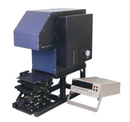
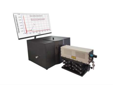
- Photosynthesis Measurement System
- Viscometer and Accessory
- Plant measuring instrument
- Fat Analyzer
- Rheometer
- Polarimeter
- Refractometer
- Flowmeter
- Colorimeter
- Multimeter
- Profilometer
- Moisture Equipment
- Ion Meter
- Dissolved Oxygen Meter
- Densitometer
- Flame Photometer
- Particle Counter
- Calibration Weight
- Stroboscope
- Conductivity Meter
- Stress Meter
- Tensiometer and Accessory
- Haze Meter
- Alcohol Meter
- Kjeldahl Nitrogen Analyzer
- Particle Analyzer
- Surface Analyzer
- Liquid Analyzer and Accessory
- Balance and Scale
- Blotting Equipment
- Electrophoresis
- Cell Analysis
- Cell Culture
- Chromatography
- Cleanroom
- Genomics Tool
- Laboratory Centrifuge
- Pipette
- Mass Spectrometry
- Microarray Equipment
- Laboratory Equipment for Animal Research
- PCR Equipment
- Spectrophotometry
- Spectroscopy
- Microscope
- Histology Equipment
- General Laboratory Equipment
- Autoclave Sterilizer
- Workspace Essentials (MRO)
- Computer System & Printer
- Consumables
- Desiccator
- Dispenser
- Electrode
- Filtration Device
- Homogenizer / Sonicator and Accessory
- Laboratory Furniture
- Laboratory Hoods (Laminar Flow Hoods / Biosafety Cabinets)
- Laboratory Scales / Scientific Balances
- Laboratory Washer
- Laboratory Water Purification / Laboratory Water System
- Storage Device
- Vacuum Centrifuge / Concentrator
- Vacuum System, Pump & Manifold and Accessory
- Vortexer and Accessory
- Chemical Synthesizer
- Power Supply
- Basic Glove Box
- Software / App / Library
- Disperser
- Furnace
- Data Logger
- Stirrer and Accessory
- Sealer
- Anti-static Device
- Torch
- Reactor System and Accessory
- Nebulizer
- Gas Regulator
- Mill and Grinder
- Accessories for Laboratory Rockers and Shakers
- Evaporator
- Digital Burette
- pH Electrodes
- Sterilizer
- Crimper and Decapper
- Probe
- Timer
- Coater and Accessory
- Ice Maker and Dry Ice Maker
- Freeze Dryers
- Sample Preparation
- Digester
- Vibrating Screen
- Accessories for Vacuum Systems, Pumps & Manifolds
- Generator
- Nitrogen Blower
- Material Mechanics Testing Machine
- Emulsification Tank
- Dry Ice Blast Cleaning
- Magnet and Magnetic Tool
- Soxhlet Extractor
- Ultrasonic Equipment
- Air Handling Equipment
- Temperature Control Equipment
- Monitoring Equipment
- Transmitter
- Gloves, Glasses and Safety
- Bag
- Controlled Environment and Cleanroom
- Ear Plug and Hearing Protection
- Eyewash and Shower
- Glasses, Goggles and Face Masks
- Glove
- Hat and Helmet
- Hazardous Materials Storage and Disposal
- Lab Coat, Apron and Apparel
- Radiation Monitoring Instrumentation
- Sharps Container
- Spill Control and Containment
- Wipe and Absorbent Pad
- Liquid Nitrogen Container
- Splash Shield
- Laser Safety Window
- Hand Sanitizer
- Lab Automation / High-Throughput
- Automated Liquid Handling Systems
- Automated DNA/RNA/Protein Purification Systems
- Automated Microplate Handling System
- Automated Solid Phase Extraction (SPE) Systems
- Dispensing Systems
- Microplate Handling (High-Throughput/Automation)
- Microplate Handling (Low / Medium Throughput/Automation)
- Microplate Washer
- Multipurpose Workstation
- Automated Cell Culture Systems
- Workstation Module
- Aspiration System
- Pumps and Dispensing Equipment
- High Throughput Screening System
- Automated Molecular Diagnostic Instrument
- Automation Reservoir
- Filler-Liquid
- Robot Arm
- Labware
- Filtration Consumable
- Cryo-preservation Consumable
- Sampling Tool
- Microplate and Plate Seal
- Staining Appliance
- Container
- Weighing and Measuring Appliance
- Stopper, Plug and Lid
- Bottle, Tube, Vessel and Vial
- Indicator Paper
- Liner and Mat
- Lab Cleaning Supply
- Lab Organization Supply
- Valve and Stopcock
- Lab Tubing
- Flask and Beaker
- Adapter
- Connector
- Sealing
- Funnel
- Condenser
- Distiller
- Trap
- Syringe and Syringe Needle
- Grinder Tool
- Jack and Jack Accessory
- Dish
- Spray Chamber
- Liquid Transfer Accessory
- Fixing Tool
- Other Lab Supply
- Autoradiography Film
- Sublimation Apparatus
- Tweezer, Scissor and Cutter
- Bubbler
- NMR Tube and Accessory
- Mantle
- RF Coil
- Extraction Thimble
- Fritted Disc
- Clamp and Clip
- Molecular Model
- Crucible and Accessory
- Extractor
- Tag
- Buret
- Support and Stand
- Filling Bell
- Bead
- Dialysis Membrane
- Cover Glass
- Kettle
- Micro Capillary
- Anti-Climb
- Gas Dispersion Tube
- Gas Washing Bottle
- Shovel
- Wire Gauze
- Hook
- Sample Transport Packaging
- Mesh Netting
- Ports & Sparger
- Glass Kiln
- Test Strip Cassette
- Dialysis Chamber
- Insect Container
- Lab Furniture
- Microfluidic Equipment
- Cell Therapy
- Optical Elements
- Wearable
- Materials
- 3D Printing
- Analytical Instrumentation / Analytical Equipment
-
- Active Surgical Instrument
- Passive Surgical Instrument
- Knife
- Surgical Scissor
- Surgical Instrument-Forcep
- Surgical Instrument-Needle
- Surgical Instrument-Hook
- Surgical Instrument-Curette
- Surgical Instrument-Retractor
- Surgical Instrument-Puncture Guidance
- Surgical Instrument-Stapling Instrument and Material
- Surgical Instrument-Procedure Kit
- Surgical Instrument-Handle and Sheath
- Surgical Instrument-Spoon
- Surgical Instrument-Clamp
- Surgical Instrument-Grasper
- Other Surgical Instrument
- Radiotherapy Equipment
- Medical Imaging Equipment
- Medical Equipment Sterilization Equipment
- Blood Transfusion, Dialysis and Extracorporeal Circulation Equipment
- Blood Separation, Treatment, Storage Equipment
- Blood Separation, Treatment, Storage Appliance
- Blood Purification and Peritoneal Dialysis Equipment
- Blood Purification and Peritoneal Dialysis Appliance
- Cardiopulmonary Circulation Equipment
- Cardiopulmonary Circulation Appliance
- Blood Management Software
- Medical Examination and Monitoring Equipment
- Diagnostic Aid
- Respiratory Function and Gas Analysis and Measurement Device
- Physiological Parameter Analysis and Measurement Equipment
- Monitoring Equipment
- Radionuclide Diagnostic Equipment
- Ultrasound Physiological Parameter Measurement and Analysis Equipment
- Telemetry and Central Monitoring Equipment
- Other Measurement and Analysis Equipment
- Nursing Station Equipment
- Respiration, Anesthesia and First Aid Equipment
- Physical Therapy Equipment
- Active Implant
- Passive Implant Device
- Osteosynthesis Implant
- Reconstruction and Replacement of Sport Injury Soft Tissue Implant
- Spinal Implant
- Joint Replacement Implant
- Orthopaedic Filling and Repair Material
- Implant in Neurology, Neurosurgery
- Cardiovascular Implant
- Orthopedic and General Surgical Implant
- Tissue Engineering Scaffold Material
- Other Passive Implant Device
- Stent
- Patient-Carrying Instrument
- Ophthalmic Instrument
- Oral Instrument
- Obstetrics and Gynecology, Assisted Reproduction, Contraceptive Device
- Medical Rehabilitation Apparatus
- Clinical Test Equipment
- Blood Analysis Equipment
- Biochemical Analysis Equipment
- Electrolyte and Blood Gas Analysis Equipment
- Immunoassay Equipment
- Molecular Biology Analysis Equipment
- Microbial Analysis Equipment
- Scanning Image Analysis System
- Radionuclide Specimen Measuring Device
- Urine and Other Sample Analysis Equipment
- Other Medical Analysis Equipment
- Sampling Equipment and Appliance
- Sample Processing Equipment before Morphological Analysis
- Sample Separation Equipment
- Culture and Incubation Equipment
- Inspection and Other Auxiliary Equipment
- Medical Biological Protection Equipment
- Orthopedic Surgery Instrument
- Neuro and Cardiovascular Surgery Instrument
- Infusion, Nursing and Protective Equipment
- Injection, Puncture Apparatus
- Intravascular Infusion Apparatus
- Non-Vascular Transfusion Device
- Hemostatic Device
- Non-Vascular Catheter
- Extracorporeal Device for Use with Non-Vascular Catheter
- Absorbable Surgical Dressing
- Non-absorbable Surgical Dressing
- Wound Dressing
- Stoma, Scar Care Product
- Operating Room Infection Control Supply
- Medical Staff Protective Equipment
- Patient Care Protective Gear
- Other Equipment
- Brain-Computer Interface
- Medical Furniture
- Medical Furniture
-
-
-
- Genomics Technology
- Cytogenetics Technique
- Proteomics Technology
- Metabolomics Technology
- Protein Expression / Antibody Customization
- Protein Purification Technology
- Gene / Protein Microarray
- Immunoassay Technology
- PCR Technology
- Enzyme-Linked Immunosorbent Assay (ELISA) Technology
- MSD Hypersensitive Multi-Factor Electrochemiluminescence Technology
- Cytokine and Signaling Pathway Assay
- Fluorescence Recovery After Photobleaching (FRAP) Technology
- Amino Acid Analysis Technology
-
- Flash Photolysis Technique
- Ultrafast Laser Spectroscopy
- Optoacoustic Spectroscopy
- Dielectric spectroscopy
- Spectral Karyotype (SKY) Technique
- NMR Spectroscopy Technology
- Diffusing Wave Spectroscopy (DWS) Technology
- UV-Vis Spectroscopy Technology
- Electron Paramagnetic Resonance (EPR) Spectroscopy Technology
- Fluorescence Correlation Spectroscopy (FCS) Technology
- Circular Dichroism (CD) Technology
- Dynamic and Static Light Scattering (DLS / SLS) Technology
- Near Infrared (NIR) Spectroscopy Technology
- Frequency Modulation Spectroscopy (FMS) Technology
- Raman Spectroscopy Technology
- Accelerator Mass Spectrometry (AMS) Technology
- Linear Dichroism (LD) Technology
- Atomic Spectrometry Technology
- X-Ray Spectrometry Technology
- Secondary Ion Mass Spectrometry (SIMS) Technology
- Scattering Spectroscopy Technology
- Isotope Ratio Mass Spectrometry (IRMS)
- Ion Mobility Spectrometry–Mass Spectrometry (IMS-MS)
- Thermal Ionization Mass Spectrometry (TIMS)
- Spark Source Mass Spectrometry (SSMS)
- Matrix Assisted Laser Desorption Ionisation-Time of Flight (MALDI-TOF) Mass Spectrometry
- Surface Enhanced Laser Desorption Ionization-Time of Flight (SELDI-TOF) Mass Spectrometry
-
- Liquid Chromatography - Mass Spectrometry (LC-MS) Technology
- Liquid Chromatography-Charged Aerosol Detection (LC-CAD) Technology
- Reversed-Phase Chromatography (RP-HPLC / RP-UPLC) Technology
- Gas Chromatography-Mass Spectrometry (GC-MS) Technology
- Paper Chromatography Method
- High-Performance Liquid Chromatography (HPLC) Technology
- Ion-Exchange Chromatography (IEX) Technology
- Thin Layer Chromatography (TLC) / High-Performance Thin Layer Chromatography (HPTLC) Technology
- Supercritical Fluid Chromatography Technology
- Affinity Chromatography Method
-
- Kinetic Exclusion Assay (KinExA) Technology
- Bio-Layer Interferometry (BLI) Technology
- Quartz Crystal Microbalance (QCM) / Dissipation (QCM-D) Technology
- Surface Plasmon Resonance (SPR) Technology
- Dual Polarization Interferometry (DPI) Technology
- Differential Scanning Calorimetry (DSC) Technology
- Microscale Thermophoresis (MST) Technology
- Isothermal Titration Calorimetry (ITC) Technology
- Differential Scanning Fluorimetry (DSF) Technology
-
- Animal Behavior Experiment
- Construction of Animal Disease Model
- Orthopedic Animal Model
- Organ Transplantation Animal Model
- Nervous System Animal Model
- Dermatology Animal Model
- Cardiovascular and Cerebrovascular Animal Model
- Respiratory System Animal Model
- Digestive System Animal Model
- Urinary System Animal Model
- Endocrine System Animal Model
- Five-sense Disease Animal Model
- Tumor Animal Model
- Other Animal Model
- Genetically Modified Animal
- In Vivo Pharmacodynamic Evaluation
-
- Capillary Electrophoresis (CE) Technology
- Polyacrylamide Gel Electrophoresis (PAGE) Technology
- Blue Native Polyacrylamide Gel Electrophoresis (BN-PAGE) Technology
- Sodium Dodecyl Sulfate Polyacrylamide Gel Electrophoresis (SDS-PAGE) Technology
- Two-dimensional Polyacrylamide Gel Electrophoresis (2-DE / 2D-PAGE) Technology
- Agarose Gel Electrophoresis (AGE) Technology
- Cellulose Acetate Electrophoresis (CAE) Technology
- Isoelectric Focusing (IEF) Technology
-
- Viscosity Testing Technique
- Distillation Range Testing Technique
- Boiling Point Testing Technique
- Melting Point Testing Technique
- Moisture Measurement Technique
- Conductivity Measurement Technology
- Thermal Conductivity Measurement Technology
- Determination of Approximate PH of Solution
- Determination of Clarity and Degree of Opalescence of Liquid
- Determination of Degree of Coloration of Liquid
- Determination of Total Organic Carbon in Water for Pharmaceutical Use
- Determination of Freezing Point
- Determination of Drop Point
-
-
-
- Analytical Balance and Accessory
- Chemistry Analyzer
- Fluorometer / Fluorescence Detection Instrument
- Other Analytical Instrument - Analytical Equipment
- Particle Analyzer
- pH Meter and Osmometer
- Testing & Inspection Machine
- Sample Preparation Equipment
- Pressure Testing / Analysis Equipment
- Viscometer and Accessory
- Rheometer
- Polarimeter
- Refractometer
- Flowmeter
- Colorimeter
- Multimeter
- Profilometer
- Densitometer
- Flame Photometer
- Particle Counter
- Conductivity Meter
- Tensiometer and Accessory
- Moisture Equipment
- Calibration Weight
- Spectrum Analyzer
- Network Analyzer
- Communication Analyzer
- Test Set
- Frequency Counter
- Signal Generator
- Other Electronic Test Equipment
- Power Meter
- Voltmeter
- Balance and Scale
- Surface Analyzer
-
- Computer System & Printer
- Desiccator
- Dispenser
- Filtration Device
- Homogenizer / Sonicator and Accessory
- Laboratory Furniture
- Laboratory Hood (Laminar Flow Hood / Biosafety Cabinet)
- Laboratory Scales / Scientific Balances
- Laboratory Washer
- Laboratory Water Purification / Laboratory Water System
- Storage Device
- Vacuum Centrifuge / Concentrator
- Vacuum System, Pump & Manifold and Accessory
- Vortexer and Accessory
- Chemical Synthesizer
- Basic Glove Box
- Disperser
- Reactor System
- Gas Regulator
- Mill and Grinder
- Evaporator
- Sterilizer
- Probe
- Ice Maker and Dry Ice Maker
- Ultrasonic Cleaner
- Generator
- Food Dehydrator
- Software / App / Library
- Imager and Scanner
- Laser and Accessory
- Sealer
- Power Supply
- Light Source and Lamp
- Lab Miscellaneous
- Lab Mixer and Stirrer
- Temperature Control Equipment
- Air Handling Equipment
- Monitoring Equipment
-
- Automated Microplate Handling System
- Microplate Washer
- High Throughput Screening System
- Filler-Liquid
- Robot Arm
- Automated Sample Preparation System
- Microplate Stacker
- Labeler
- Robotics
- Other Lab Automation
- Lab Automation Accessory
- Packing Equipment
- Deduster
- Lifter
- Conveyor
- Palletizer
- Tank
- Metal Detector
- Feeder
-
-
-
- Pharmaceutical Service
- Filter Equipment Testing
- Automobile Testing
- Daily Chemical Testing
- Electronic and Electrical Testing
- Soil Testing
- Metal Material Testing
- Gemstone and Treasures Identification
- Metallurgical Testing
- Surface Modification Service
- Chemical Product Testing
- Solid Waste Testing
- Food Testing
- Disinfection and Sterilization Product Testing
- Water Testing
- Gas Testing
- Polymer Testing
- Construction Material Testing
- Air Purification Material Testing
-
- Microfluidics Application
- Microfluidics for Food Testing
- Microfluidics for Biomanufacturing
- Microfluidics for Pharmaceutical Research
- Microfluidics for Environmental Monitoring
- Microfluidics for Single-Cell Analysis
- Microfluidics for Cell Sorting and Separation
- Microfluidics for Nucleic Acid Amplification
- Microfluidics for Microparticle Synthesis
- Microfluidics for Microfiber Synthesis
- Microfluidics for Emulsion Synthesis
- Microfluidics for Microbial Research
- Organ-on-a-Chip
- Microfluidic Device Development and Manufacturing
- Microfluidics Application
-
- Nanoparticles Functionalization and Modification
- Nanoparticles Synthesis
- Application Development of Nanoparticles
- Nanoparticles Development for Biomedical Applications
- Nanoparticles Development for Electronic Applications
- Nanoparticles Development for Environmental Applications
- Nanoparticles Development for Energy Storage and Conversion
- Nanoparticles Development for Agricultural Applications
- Nanoparticles Development for Food Applications
- Nanoparticles Development for Cosmetics and Personal Care Applications
- Nanoparticle Characterization
- Elemental Composition Determination
- Molecular Composition Determination
- Particle Size and Distribution Analysis
- Shape Determination
- Crystal Structure Analysis
- Oxidation State Analysis
- Surface Properties Characterizations
- Agglomeration State Analysis
- Optical Properties Characterization
- Magnetic Properties Characterization
- Toxicity Evaluation
- Structural Defects Detection
-
- Protective Barriers & Material Performance
- Antimicrobial Efficacy Studies
- Bacterial & Viral Filtration Efficacy (BFE/VFE) Test
- Hydrostatic Pressure Test
- Microbial Cleanliness
- Partible Filtration Efficiency (PFE) Test
- Spray Impact Test
- Synthetic Blood Penetration Test
- Tensile and Tear Resistance Tests
- Flammability Test
- Viral Penetration Test
- Glove Testing
- Gown Testing
- Face Mask Testing
- Eyewear Testing
- Safety Footwear Testing
- Protective Barriers & Material Performance
-
- Mechanical Properties Test
- Corrosion Testing
- Physical Properties Test
- Electrical Properties Test
- Optical Properties Test
- Structural Characterization
- Thermal Analysis
- Non-Destructive Testing
- Chemical Analysis
- Surface and Morphology Analysis
- Metallurgical Analysis
- Grain Size Analysis
- Carburization and Decarburization Determination
- Heat Treatment Metallurgy
- Surface Contamination Testing
- Metallurgical Failure Analysis
- Macro-Etching Examination
- Nodularity Measurement
- Grain Flow Analysis
- Case Depth Measurement
- Inclusion Rating
- Ferrite Testing
- Coating Testing
- Weld Testing
- Porosity Testing
- Acoustic, Optical, Electrical and Magnetic Analysis
-
- Mass Spectrometry Clinical Diagnostics Service
- Biomarker Discovery Service Based on Targeted LC-MS/MS
- Clinical Metabolomics Service Based on HRMS
- Therapeutic Drug Monitoring Service Based on Triple Quadrupole MS
- Inborn Errors of Metabolism Screening Service Based on Tandem MS
- HCP (Host Cell Protein) Identification and Quantification Service Based on LC-MS/MS
- Quantitative Proteomics Service Based on TMT Labeling and Orbitrap MS
- Mass Spectrometry Structural Elucidation Service
- Compound Structure Identification Service Based on NMR-MS Hybrid
- Fragmentation Pattern Analysis Service Based on Ion Trap MS
- De Novo Sequencing Service Based on High-Resolution MS
- Polymer Structural Characterization Service Based on MALDI-TOF MS
- Fingerprinting and Equivalence Analysis Service Based on LC-MS/MS
- Mass Spectrometry Food and Beverage Analysis Service
- Food Contaminant Analysis Service Based on GC-MS/MS
- Flavor and Aroma Compound Identification Service Based on SPME-GC-MS
- Nutrient Quantification Service Based on LC-MS/MS
- Adulteration Detection Service Based on HRMS
- Food Authenticity Verification Service Based on Isotope Ratio Mass Spectrometry (IRMS)
- Mass Spectrometry Material Science and Polymer Analysis Service
- Polymer Characterization Service Based on MALDI-TOF MS
- Surface Analysis Service Based on SIMS
- Molecular Weight Determination Service Based on Gel Permeation Chromatography (GPC) coupled with MS
- Degradation Product Analysis Service Based on LC-MS
- Stability Testing Service Based on LC-MS/MS and GC-MS/MS
- Phthalates and Alkylphenols Detection Service Based on LC-MS/MS
- Mass Spectrometry Protein and Peptide Analysis Service
- Mass Spectrometry Metabolomics Service
- Targeted Metabolomics Service Based on Triple Quadrupole MS
- Untargeted Metabolomics Service Based on High-Resolution MS (HRMS)
- Lipidomics Service Based on Orbitrap MS
- Metabolite Identification Service Based on GC-MS
- Phospholipid Analysis Service Based on HILIC-LC-MS
- Glycomics Analysis Service Based on MALDI-TOF MS
- Mass Spectrometry Drug Discovery and Pharmacokinetics Service
- Drug Metabolism Service Based on LC-MS/MS
- Pharmacokinetic Analysis Service Based on Triple Quadrupole MS
- Bioavailability Study Service Based on LC-MS/MS
- Quantitative Bioanalysis Service Based on LC-MS/MS
- Biomarker Quantification Service Based on PRM Scanning with Orbitrap MS
- DMPK Analysis Service Based on UPLC-MS/MS
- Mass Spectrometry Environmental Analysis Service
- Trace Organic Pollutants Detection Service Based on GC-MS/MS
- Pesticide Residue Analysis Service Based on LC-MS/MS
- Heavy Metal Analysis Service Based on ICP-MS
- Volatile Organic Compounds (VOCs) Analysis Service Based on GC-MS
- Extractables and Leachables Testing Service Based on High-Resolution GC-MS/MS
- Mass Spectrometry Clinical Diagnostics Service
-
- Scanning Electron Microscopy (SEM) Service
- Atomic Force Microscopy (AFM) Service
- Correlative Microscopy Service
- Spectroscopy and Imaging Combination Service
- Chemical Imaging Service Based on Horiba XploRA Plus Confocal Raman Microscope
- Tip-Enhanced Raman Spectroscopy (TERS) Service Based on Renishaw InVia Raman Microscope
- Molecular Interaction Analysis Service Based on Leica SP8 FALCON FLIM System
- FLIM for Live-Cell Imaging Based on Zeiss LSM 980 with Airyscan 2
- High-Resolution Imaging Service
- STED Microscopy Service Based on Leica STED Super-Resolution Microscope
- SIM Microscopy Service Based on Nikon Structured Illumination Microscopy
- PALM/STORM Service Based on Zeiss ELYRA PS.1 System
- Confocal Imaging Service Based on Leica SP8 Confocal Microscope
- Live Cell Imaging Service Based on Olympus FV3000 Confocal System
- Multicolor Confocal Imaging Service Based on Zeiss LSM 980 System
- Ultrastructure Analysis Service Based on JEOL JEM-2100 TEM
- Cryo-TEM Service Based on FEI Tecnai G2 Cryo-TEM
- High-Resolution TEM Service Based on Thermo Fisher Talos TEM
- 3D Imaging and Tomography Service
- 3D Volume Reconstruction Service Based on ZEISS Sigma SBF-SEM
- High-Resolution 3D Surface Analysis Service Based on FEI Quanta 3D FIB-SEM
- Nanoscale 3D X-ray Imaging Service Based on Zeiss Xradia 810 Ultra
- Micro-CT Service Based on Bruker SkyScan Micro-CT
- Cellular and Molecular Structure Analysis Service Based on Thermo Fisher Krios Cryo-EM
- Cryo-ET for Biological Samples Based on JEOL CryoARM 300
- Fluorescence and Light Microscopy Service
- High-Content Screening Service Based on PerkinElmer Operetta CLS
- Fluorescence Imaging Service Based on Nikon Eclipse Ti2
- Deep Tissue Imaging Service Based on Zeiss LSM 880 NLO Multiphoton Microscopy
- 3D Live Imaging Service Based on Olympus FV1000 Multiphoton Microscope
- Large-Scale Tissue Imaging Service Based on Zeiss Lightsheet Z.1
- High-Speed Light Sheet Imaging Service Based on Leica TCS SP8 DLS
-
- Flow Cytometry Sample Preparation and Processing Service
- Flow Cytometry Specialized Analytical Service
- Immunophenotyping Service Based on Flow Cytometry Systems
- Receptor Occupancy Service Based on Flow Cytometry Systems
- Functional Assays Service Based on Flow Cytometry Systems
- Cell Cycle Analysis Service Based on Flow Cytometry Systems
- Apoptosis Detection Service Based on Flow Cytometry Systems
- Cytokine Production Analysis Service Based on Flow Cytometry Systems
- Phosphoflow Service Based on Flow Cytometry Systems
- Intracellular and Cell Surface Antigens Service Based on Flow Cytometry Systems
- Cellular Activation and Immune Checkpoint Analysis Service Based on Flow Cytometry Systems
- Immune Function Analysis Service Based on Flow Cytometry Systems
- Rare Cell Detection Service Based on Flow Cytometry Systems
- Multi-Parameter Phenotype Analysis Service Based on Flow Cytometry Systems
- Histone Methylation Analysis Service Based on Flow Cytometry Systems
- Real-Time Flow Cytometry Service Based on Flow Cytometry Systems
- Cell Enumeration Service Based on Flow Cytometry Systems
- Cellular Phenotyping Service Based on Flow Cytometry Systems
- Cellular Proliferation and Cell Cycling Service Based on Flow Cytometry Systems
- Spectral Flow Cytometry Service Based on Spectral Flow Cytometry Systems
- MDSC Assays Service Based on Flow Cytometry Systems
- DNA Content Analysis Service Based on Flow Cytometry Systems
- Cellular Calcium Level Analysis Service Based on Flow Cytometry Systems
- Mitochondrial Membrane Potential Analysis Service Based on Flow Cytometry Systems
- Mass Cytometry Analysis Service Based on Mass Cytometry Systems
- Flow Cytometry Cell Sorting and Analysis Service
- Flow Cytometry Quality Control and Data Processing Service
-
- Hydrogel Wound Dressing Development Service
- Hydrogel Contact Lens Development Service
- Hydrogel Sensor Development Service for Biomonitoring
- Blood Glucose Hydrogel Sensor
- Biomarker Hydrogel Sensor
- Ion-Sensitive Hydrogel Sensor
- Temperature-Sensitive Hydrogel Sensor
- Muscle Movement Hydrogel Sensor
- Heart Rate Monitoring Hydrogel Sensor
- Hydrogel Sensor for Infectious Disease Surveillance
- Respiratory Monitoring Hydrogel Sensor
- Sweat Monitoring Hydrogel Sensor
- Hydrogel Scaffold Development Service for Tissue Engineering
- Hydrogel Scaffolds for Cardiac Tissue Engineering
- Hydrogel Scaffolds for Vascular Tissue Engineering
- Hydrogel for Bone Tissue Engineering
- Hydrogel Scaffolds for Cartilage Tissue Engineering
- Hydrogel Scaffolds for Pancreatic Tissue Engineering
- Hydrogel Scaffolds for Nervous Tissue Engineering
- Hydrogel Scaffolds for Eye Tissue Engineering
- Hydrogel Scaffolds for Skin Tissue Engineering
- Hydrogel Scaffolds for Oral Tissue Engineering
- Hydrogel Scaffolds for Liver Tissue Engineering
- Hydrogel-based Hygiene Product Development Service
- Hydrogel Drug Delivery System Development Service
- Hydrogel-based Dermal Filler Development Service for Facial Correction
- Hydrogel Coating Development Service for Medical Device
- Hydrogel Cosmetic Product Development Service
- Hydrogel‐based Embolic Agent Development Service
- Hydrogel-based Radioprotective Spacer Development Service
-
- Plant Nutrition
- Detection of Amino Acids in Plant Tissues
- Detection of Pectin in Plant Tissues
- Detection of Sugars in Plant Tissues
- Detection of Cellulose in Plant Tissues
- Detection of Organic Acids in Plant Tissues
- Detection of Naphthoquinones in Plant Tissues
- Detection of Alkaloids in Plant Tissues
- Detection of Vitamins in Plant Tissues
- Detection of Fatty Acids in Plant Tissues
- Detection of Lignin in Plant Tissues
- Detection of Saponins in Plant Tissues
- Detection of Volatile Oil in Plant Tissues
- Detection of Flavonoids in Plant Tissues
- Detection of Plant Respiration
- Evaluation of Plant Photosynthesis
- Plant Hormone Detection
- Plant Elements Determination
- Plant Pigment Detection
- Plant Immunity
- Plant Nutrition
-
- Fruit Fly (Drosophila) Model Service
- Gene Knockdown Service Based on RNAi Technology in Drosophila
- Drosophila Lifespan Analysis Service Based on Automated Monitoring Systems
- Neurodegenerative Disease Service Based on Drosophila Alzheimer's and Parkinson's Models
- Behavioral Genetics Service Based on High-Speed Video Tracking of Drosophila
- Drosophila Metabolism Analysis Service Based on Respirometry and Feeding Assays
- Developmental Biology Service Based on Embryo Microinjection
- Drosophila Cardiovascular Disease Model Service Based on Pacing-Induced Heart Failure Models
- Mouse Model Service
- Transgenic Mouse Generation Service Based on CRISPR-Cas9 Technology
- Knockout Mouse Generation Service Based on Embryonic Stem Cell Technology
- Conditional Knockout Mouse Service Based on Cre-LoxP Technology
- Humanized Mouse Model Service Based on Xenografting Techniques
- Tumor Mouse Model Service Based on Orthotopic and Subcutaneous Injection Techniques
- Pharmacokinetics Service Based on In Vivo Drug Administration and Blood Sampling Techniques
- Immunotherapy Service Based on PD-1/PD-L1 Knockout Mice
- Infectious Disease Service Based on Pathogen Challenge Models
- Cardiovascular Disease Service Based on Aortic Banding Surgery
- Zebrafish Model Service
- Genetic Mutation Service Based on CRISPR-Cas9 Technology
- Zebrafish Embryo Toxicity Testing Service Based on High-Throughput Screening Platforms
- Neurodevelopmental Studies Service Based on Zebrafish Optogenetics Equipment
- Cardiotoxicity Service Based on Fluorescent Imaging and Microinjection Techniques
- Behavioral Phenotyping Service Based on Automated Video Tracking Systems
- Zebrafish Tumor Model Service Based on Cancer Cell Microinjection
- Zebrafish Regeneration Model Service Based on Tail Fin Amputation Technique
- Fruit Fly (Drosophila) Model Service
-
- Advanced Multi-Dimensional NMR Service
- Kinetic and Reaction Mechanism Study Service
- Metabolomics and Biomolecular Screening Service
- Structural Determination and Analysis Service
- 1D Proton NMR Service Based on 400 MHz Spectrometer
- 13C, 15N, 31P NMR Service Based on 500 MHz Spectrometer
- Multinuclear (1H, 13C, 15N) 2D NMR Service Based on 600 MHz Spectrometer (e.g., HSQC, HMBC)
- Natural Product Structure Elucidation Service Based on 600 MHz Spectrometer for Mass-Limited Samples
- Macromolecular Structure Determination Service Based on 700 MHz Spectrometer
- 3D NMR Service for Protein Structure Analysis Based on 800 MHz Spectrometer
- Quantitative NMR (qNMR) Service
- Bio-Molecular and Structural Biology NMR Service
- Protein-Ligand Interaction NMR Service Based on 700 MHz Spectrometer
- Metabolomics NMR Profiling Service for Biofluids (e.g., Urine, Blood) Based on 600 MHz Spectrometer
- Fragment-Based Drug Screening NMR Service Based on 500 MHz Spectrometer
- Dynamic and Conformational Study Service for Proteins Based on 800 MHz Spectrometer
- Solid-State NMR Service
- Solid-State Magic Angle Spinning (MAS) NMR Service Based on 500 MHz Spectrometer
- Cross Polarization (CP) MAS NMR Service Based on 400 MHz Spectrometer
- Structural Characterization of Polymers by Solid-State NMR Based on 600 MHz Spectrometer
- High-Speed MAS NMR for Materials with Al-Free Probe Based on 300 MHz Spectrometer
- Diffusion-Ordered Spectroscopy (DOSY) NMR Service
-
-
- BioChip Technology
- Surface Plasmon Resonance (SPR)
- Droplet Technology
- Western Blot Technology
- Polymerase Chain Reaction (PCR)
- Gene Mapping
- Recombinant DNA Technology
- Techniques for the Study of Gene Function
- Molecular Hybridization
- Molecular Interaction
- Sequence Analysis
- Genomic Library and cDNA Library
- mRNA Differential Display PCR (mRNA DD-PCR)
- RNA interference (RNAi)
- Gene Chip Technology
- Chromatin Immunoprecipitation Assay (ChIP)
- Phage Display Technology
- Protein Expression and Purification Technology
- His-Tag Protein Purification
- Antibody Preparation and Purification Technology
- Bicinchoninic Acid (BCA) Assay
- Enzyme Linked Immunosorbent Assay (ELISA)
- Bimolecular Fluorescence Complementation
- Immunohistochemistry (IHC)
- GST Pull-Down
- Protein Chip
- Footprinting
- Yeast Two-Hybrid System
- Cell Culture Technology
- Flow Cytometry (FCM)
-
- Gas Chromatography Technology
- Ion-Exchange Chromatography Technology
- Liquid Chromatography Technology
- Supercritical Fluid Chromatography Technology
- Column Chromatography Technology
- Paper Chromatography Technology
- Thin Layer Chromatography Technology
- Adsorption Chromatography Technology
- Partition Chromatography Technology
- Size Exclusion Chromatography Technology
- Affinity Chromatography Technology
-
Inquiry Basket
There is no product in the shopping cart.